


 View fulltext
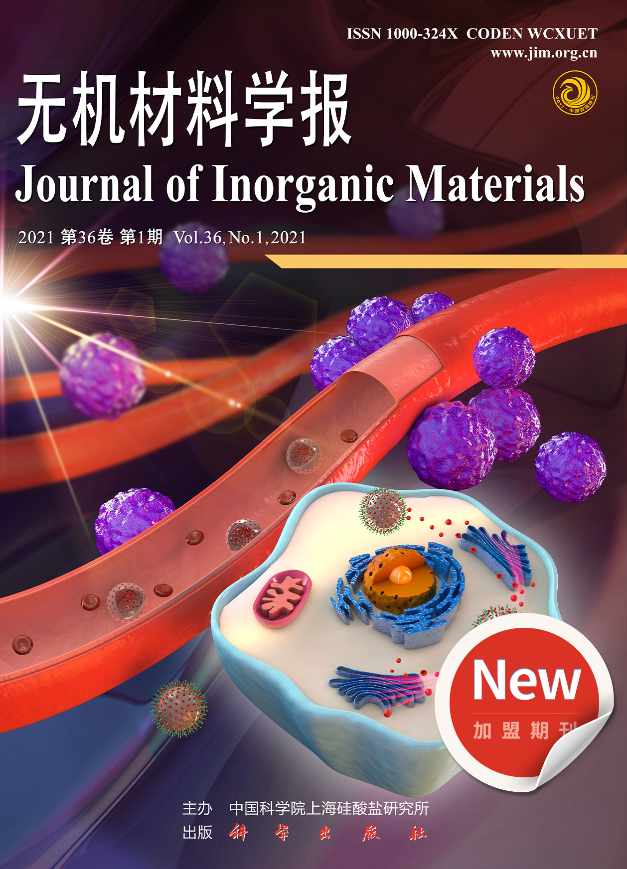

2023
Volume: 38 Issue 3
18 Article(s)

Dongfeng XUE, Liangbi SU, and Jun XU
Mar. 20, 2023Vol. 38 Issue 3 225 (2023)
Chaoyi ZHANG, Huili TANG, Xianke LI, Qingguo WANG, Ping LUO, Feng WU, Chenbo ZHANG, Yanyan XUE, Jun XU, Jianfeng HAN, and Zhanwen LU
Since the beginning of the 21st century, the third generation wide band gap (Eg>2.3 eV) semiconductor materials represented by gallium nitride (GaN) and zinc oxide (ZnO) are becoming the core supporting materials for development of semiconductor industry. Due to difficult growth and high cost of GaN and ZnO single crystal, epitaxial technology is always used as the substrate materials to grow GaN and ZnO films. Therefore, it is crucial to find an ideal substrate material for the development of third generation semiconductor. Compared with traditional substrate materials, such as sapphire, 6H-SiC and GaAs, scandium magnesium aluminate (ScAlMgO4) crystal, as a new self-peeling substrate material, has attracted much attention because of its small lattice mismatch rate (~1.4% and ~0.09%, respectively) and suitable thermal expansion coefficient with GaN and ZnO. In this paper, based on structure of ScAlMgO4 crystal, the unique trigonal bipyramid coordination and natural superlattice structure, the basis for its thermal and electrical properties, are introduced in detail. In addition, the layered structure of ScAlMgO4 crystal along the c-axis makes it self-peeling, which greatly reduces its preparation cost and has a good application prospect in the preparation of self-supported GaN films. However, the raw material of ScAlMgO4 is difficult to synthesize, and the crystal growth method is single, mainly through the Czochralski method (Cz), and growing techniques now in China lag far behind that in Japan. Therefore, it is urgent to develop a new growth method of growing high quality and large size ScAlMgO4 crystals to break the technical barriers.
Jan. 19, 2023Vol. 38 Issue 3 228 (2023)
Zhanguo QI, Lei LIU, Shouzhi WANG, Guogong WANG, Jiaoxian YU, Zhongxin WANG, Xiulan DUAN, Xiangang XU, and Lei ZHANG
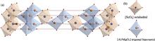
Compared with the first and second generation semiconductor materials, the third generation semiconductor materials exhibit higher breakdown field strength, higher saturated electron drift velocity, outstanding thermal conductivity, and wider band gap, suitable for manufacturing of electronic devices with high frequency, high power, radiation resistance, corrosion resistant properties, optoelectronic devices and light emitting devices. As one of the representatives of the third generation of semiconductor materials, gallium nitride (GaN) is an ideal substrate material for preparing blue-green laser, radio frequency (RF) microwave and power electronic devices. It has broad application prospects in laser display, 5G communication, phased array radar, aerospace, etc. Hydride vapor phase epitaxy (HVPE) method is the most promising method for growth of GaN crystals due to its simple growth equipment, mild growth conditions and fast growth rate. Due to the widely used quartz reactors, unintentionally doped GaN obtained by HVPE method inevitably has donor impurities (Si and O). Therefore, the grown GaN shows n-type electrical properties, high carrier concentration and low conductivity, which limits its application in high-frequency and high-power devices. Currently, doping is the most common method to improve the electrical performance of semiconductor materials, through which different types of GaN single crystal substrates can be obtained with different dopants to improve their electrochemical characteristics and meet the different needs of market applications. In this article, the basic structure and properties of GaN semiconductor crystal material are introduced, and the recent progress of the high quality GaN crystals grown by HVPE method is reviewed; and the doping characteristics, dopant types, growth process and the influence of doped atoms on the electrical properties of GaN are introduced. Finally, the challenges and opportunities faced by the HVPE method to grow doped GaN crystals are briefly described, and the future developments in several directions are prospected.
Jan. 17, 2023Vol. 38 Issue 3 243 (2023)
Kunfeng CHEN, Qianyu HU, Feng LIU, and Dongfeng XUE
Large-sized crystalline materials are the basic raw materials in semiconductors, lasers, and communications. Preparation of large-scale, high-quality crystalline materials has become a bottleneck restricting the development of related industries. Breaking through the preparation theory and technology of large-sized crystal materials is the key to obtaining high-quality large-sized crystals. Preparation process of crystal materials often undergoes nucleation and growth stages, including multiple processes at spatiotemporal scale: from atom/molecules, through clusters and nuclei, to bulk crystals. To further explore and accurately understand the crystal growth mechanism, we need intensively study the multiscale process,multi-scale in situ characterization techniques, and computational simulation methods. Among them, the latest in situ characterization methods for crystal growth includes optical microscopy, electron microscopy, vibration spectra, synchrotron radiation, neutron technology, and especially, machine learning method. Thus, the multi-scale computational simulation techniques for crystallization is introduced, for example, first principles calculation at atom/molecular scale, molecular dynamics simulation, Monte Carlo simulation, phase field simulation at mesoscopic scale, and finite element simulation at macroscopic scale. A single in situ characterization or simulation technique can only explore crystallization information over a specific time and space scale. To accurately and fully reflect the crystallization process, a combination of multi-scale methods is introduced. It can be speculated that the establishment of in situ characterization technology and computational simulation methods for the actual large-sized crystal growth environment will be the future development trend, which provides an important experimental and theoretical basis for developing crystallization theory and controlling crystal quality. Furthermore, it can be deduced that the combination of in situ characterization technology with machine learning and big data technology will be the trend for large-sized crystal growth.
Jan. 19, 2023Vol. 38 Issue 3 256 (2023)
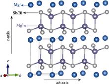
Siqi LIN, Airan LI, Chenguang FU, Rongbing LI, and Min JIN
Zintl phase Mg3X2 (X=Sb, Bi) based thermoelectric materials have attracted much attention because of their non-toxic, low cost and high performance. Compared with polycrystalline materials, the Mg3X2 crystals are of great value in revealing material’s intrinsic and anisotropic thermoelectric properties, as well as providing effective strategies for enhancing electrical and thermal transport properties. Therefore, the recent progress of single crystal growth and thermoelectric properties for Mg3X2 crystals are systematically summarizes in this paper. Due to the volatility and causticity of Mg element, several different methods such as slow cooling method, directional solidification method, flux method, and flux Bridgman method are widely used for synthesizing Mg3X2 crystals, in which the flux Bridgman method is more competitive to prepare large size bulk crystals. Researchers found that both n-type and p-type Mg3Sb2 crystals show an anisotropy thermoelectric transport property. The crystal growth rate, the concentration of self-doped Mg element, the concentration of impurity doping or alloying elements have a great impact on both electrical and thermal transport properties for Mg3Sb2 crystals. So far, the p-type and n-type Mg3Sb2 crystals with ZT value of 0.68 and 0.82 are achieved, respectively. This paper reviews the recent progress of growth and thermoelectrics properties of Zintl phase Mg3X2-based crystals, revealing that the flux Bridgman method is the most effective method to produce large-sized Mg3X2-based crystals. Tuning chemical composition of Mg3X2-based crystal by doping and forming solid solution for optimal carrier concentration and band structure engineering is expected to further improve the thermoelectric performance of Mg3X2-based crystal. The above-mentioned growth method and research strategies provide a significant guidance for the in-depth understanding of the Mg3X2-based crystal in the future.
Oct. 28, 2023Vol. 38 Issue 3 270 (2023)
Xuejun QI, Jian ZHANG, Lei CHEN, Shaohan WANG, Xiang LI, Yong DU, and Junfeng CHEN
As a multifunctional opto-electro material, Bi12GeO20 crystal shows high-speed photorefractive response in visible range, excellent piezoelectric, acousto-optic, magneto-optic, optical rotation, and electro-optic properties, etc. Presently, Czochralski (Cz) method, which is commonly used to grow Bi12GeO20 crystals, has several bottle-necks, such as high growth cost, irregular crystal boule shapes, low growth yield, poor optical quality in large crystals, and small effective crystal cross-sectional area. In this study, large Bi12GeO20 crystals were firstly grown by using modified vertical Bridgman method in platinum crucibles and air atmosphere. Morphology, distribution, and constitutes of main macroscopic defects in as-grown Bi12GeO20 crystals were investigated, and the formation process and causes of the main macroscopic defects during the crystal growth were studied. Dendrite and tubular inclusions are two types of main macroscopic defects existed in as-grown Bi12GeO20 crystals. The formation of dendrite inclusions is closely related to the platinum corrosion, while the formation of tubular inclusions is associated with precipitation of platinum, a mismatch in the stacking of growth units due to instability of the seeding interface, and instability temperature field. Technical approaches to eliminate or reduce these two types of macroscopic defects during the growth using vertical Bridgman method were proposed. High optical quality, large Bi12GeO20 crystals with sizes up to 55 mm×55 mm×80 mm and significantly improved optical transmittance were grown reproducibly by reducing control temperature, decreasing period of melt preserved at high temperature, and selecting seed crystals with better quality.
Jan. 11, 2023Vol. 38 Issue 3 280 (2023)

Honghe MU, Pengfei WANG, Yufeng SHI, Zhonghan ZHANG, Anhua WU, and Liangbi SU
With the continuous development of CeF3 crystals in laser and magneto-optical applications, the demand for CeF3 single crystals with large size and high optical quality has become increasingly urgent, while the high viscosity and low thermal conductivity of CeF3 melt always bring challenges to crystal growth process. In order to study the growth problem caused by low thermal conductivity of CeF3 melt, the influence mechanism of the furnace structure and process parameters on temperature distribution and crystallographic interface during the growth process was explored. In this work, numerical simulations about the growth of large size CeF3 crystal (ϕ80 mm) through the heat exchanger-Bridgman method were carried out to analyze the relationship between furnace structure and crystal/melt temperature distribution, the variation of interface shape in different growth stages, and the mechanism of thermal field structure on the growth interface. Results show that when the length of the heating element matches the length of the crucible, it is more conducive to construct a reasonable temperature gradient field. The unfavorable concave interface during the “shouldering” and “cylindering” growth stages can be effectively improved by adjusting temperature distribution on the ampoule wall through changing the baffle shape and adding a reflective screen. Therefore, the result not only deepens understanding of the crystallization habit of CeF3 crystals, but also enlightens the furnace and growth interface optimization of other crystals’ Bridgman growth.
Nov. 20, 2023Vol. 38 Issue 3 288 (2023)
Zhen WU, Huifang LI, Zhonghan ZHANG, Zhen ZHANG, Yang LI, Jianghe LAN, Liangbi SU, and Anhua WU
With the rapid development of high power laser and optical communication technology, how to eliminate the reflected noise generated inside the optical system is a crucial challenge. The magneto-optical isolators are magnetically active devices designed according to the Faraday effect, which can effectively isolate most of the reflected light to ensure the stable operation of the optical system. As the core component of the magneto-optical isolator, research and application of Faraday magneto-optical materials are promoting the update and development of the magneto-optical isolators. CeF3 crystals have the advantages of high transmittance, wide transmission range and high Verdet constant, and have received widespread attention in recent years for the excellent magneto-optical property. But its traditional growth methods have some disadvantages such as high cost and long cycle. In this study, multiple CeF3 crystals were successfully obtained by the porous crucible technology through optimizing the temperature field structure and process of Bridgman growth technology. Compared with commercial TGG(Tb3Ga5O12) crystals, CeF3 crystals have a significantly high transmittance up to 92%, and a comparable Verdet constant in the near-infrared wavelength, and the thermal performance test results show that CeF3 crystals have high specific heat, indicating a strong thermal shock resistance and a high laser damage resistance. Therefore, the porous crucible technology is a large-scale and low-cost production method, which can be used to grow CeF3 crystals achieving with excellent physical properties, exhibits great potential to develop magneto-optical isolators in the near-infrared band.
Dec. 30, 2023Vol. 38 Issue 3 296 (2023)
Yicun LI, Xuedong LIU, Xiaobin HAO, Bing DAI, Jilei LYU, and Jiaqi ZHU
Single crystal diamond is a kind of crystal material with excellent performance, which has important application value in advanced scientific field. In the field of single crystal diamond growth by microwave plasma chemical vapor deposition (MPCVD), improvement of crystal growth rate is still a key challenge, although corrent high energy density plasma has been a ralatively effective method. In this work, a special plasma focusing structure was designed through magnetohydrodynamic (MHD) model simulation which then was used in the growth experiment based on the simulation. The plasma properties were studied by means of spectral analysis and plasma imaging, and late on single crystal diamond samples were synthesized. The simulation results show that the core electric field and electron density under focusing conditions were 2 times higher than those under normal conditions. The growth experiment results show that plasma with high energy density (793.7 W/cm3) is obtained under conventional microwave power (3500 W) and growth pressure (18 kPa), which is consistent with the model calculation results. We find that a certain amount of nitrogen instead of high energy density growth conditions can significantly change the growth morphology and affect the quality of the crystal. With those findings, we realize the growth rate of single crystal diamond up to 97.5 μm/h. Different from the way to obtain high energy density by increasing the growth pressure, single crystal diamond can be synthesized with high energy density under normal growth pressure and microwave power.
Jan. 11, 2023Vol. 38 Issue 3 303 (2023)
Han SUN, Wenjun LI, Zixuan JIA, Yan ZHANG, Liying YIN, Wanqi JIE, and Yadong XU
Terahertz (THz) technology has immersing potential applications in industrial non-destructive testing, scientific research and military engineering. However, as the most commonly used THz emission and detection electro-optical material, the ZnTe single crystal growth still faces great challenges. In order to achieve ZnTe single crystals with large size, good homogeneity and high performance, an accelerated crucible rotation technique (ACRT) was introduced in growing ZnTe crystals by temperature gradient solution growth method (TGSG). Intrinsic ZnTe single crystals with high crystalline quality were successfully prepared. Through the simulation of flow field and solute distribution at different rotation speeds, the influence of ACRT technology on the stability of solid-liquid interface and Te inclusions distribution in crystal growth were investigated. During the crystal growth, the ACRT technology can effectively promote the melt flow, improve the solute mass transfer ability and stabilize the solid-liquid interface, which not only avoids the appearance of mixed phase zone at the crystal tail, but also reduces the number and size of Te inclusions in the crystal. With the further optimizing parameters, a large size ZnTe single crystal with a diameter of 60 mm was prepared. Meanwhile, the high response area of terahertz exceeding 90% faces due to the great uniformity of ZnTe crystal, which meant the edge effect being significantly limited and the ZnTe crystal meeting the commercial imaging requirements. Therefore, introduction of ACRT technology can provide a new strategy for preparation of ZnTe based electro-optical crystals.
Jan. 11, 2023Vol. 38 Issue 3 310 (2023)
Xiaotu SHI, Qingli ZHANG, Guihua SUN, Jianqiao LUO, Renqin DOU, Xiaofei WANG, Jinyun GAO, Deming ZHNAG, Jiandang LIU, and Bangjiao YE
In order to meet the development needs of solid-state lasers, it is necessary to continuously improve the YAG laser crystal growth technology. However, controlling the defect structure in YAG is particularly difficult for crystal development in industry and scientific research. The defects of crystal samples prepared by the two processes were studied, especially the origin of crystal scattering points. Positron annihilation technology (PAT) is a sensitive and effective nuclear technology for analysis and characterization method being used to control microstructure of materials, which is extremely sensitive to vacancy defects and micropores. According to the PAT analysis results,the positron annihilation lifetime spectrum and Doppler broadening spectrum, the positron lifetimes and line-shape parameters of Doppler broadening spectra of samples vary with different processes and with or without scattering points indicating that the main defects of the crystal are the intrinsic defects in the YAG structure.The scattering points may be nanopores caused by vacancy agglomeration, indicating that the PATis very sensitive to characterize the scattering points in the YAG crystal. The present experimental results of positron annihilation are consistent with the results of single crystal quality reflected by X-ray diffraction (XRD), single crystal rocking curve (XRC), optical transmittance, and dislocation density, indicating the uniqueness and technical advantages of positron annihilation technology in studying the relationship between physical properties and defects/microstructure of crystal materials. Meanwhile, it can be concluded that the PAT can effectively reflect the crystal quality at micro scale.
Nov. 16, 2023Vol. 38 Issue 3 316 (2023)
Xiaoming YANG, Jianghe LAN, Zhantao WEI, Rongbing SU, Yang LI, Zujian WANG, Ying LIU, Chao HE, and Xifa LONG
Yttrium iron garnet (Y3Fe5O12, YIG) crystals have been widely used in microwave and magneto-optic devices due to their excellent magnetic and magneto-optical properties. Currently, the commercial material is YIG single crystal thin films, which is deposited on Gd3Ga5O12 (GGG) substrate using liquid phase epitaxy technique. Herein, we report a new growth technology of YIG single crystal by top seeded solution growth (TSSG) technique from lead-free B2O3-BaF2 flux. The maximum size and weight of the as-grown YIG crystal can be up to 43 mm× 46 mm×11 mm and 60 g, respectively. The crystals exhibit excellent comprehensive performances with narrow ferromagnetic resonance linewidth (0.679 Oe, 1 Oe=250/π A/m), high transparency (75%) and Faraday rotation angle (200 (°)·cm-1@1310 nm and 160 (°)·cm-1@1550 nm), indicating a good candidate in microwave and magneto-optic devices. More significantly, this growth technique is ideally suited to large size YIG or doped-YIG single crystals ascombined with the oriented seed crystal and lifting process, which can significantly decrease the manufacture cost.
Oct. 25, 2023Vol. 38 Issue 3 322 (2023)
Zhiqiang WANG, Ji’an WU, Kunfeng CHEN, and Dongfeng XUE
Currently, although Er3+ and Yb3+ co-doped YAG crystals are widely used in high power solid state lasers, there are still many challenges in growing large size, low defect doped YAG crystals using the Czochralski (Cz) method. In this paper, large-sized Er3+ and Yb3+ co-doped YAG bulk crystal with a diameter of 80 mm and a length of 230 mm was obtained by the fast Cz growth method. Their structure, doping concentration, optical absorption, luminescence performances, and etching defects were evaluated.According to the Raman detecting results, there is no significant variation in the peak positions and full width at half maxima (FWHM) of the Raman peaks at different locations on the wafer, indicating that the crystal structure and strain at central and edge section of thel wafer are uniformity. The etching results show that the corrosion pits are evenly distributed over the entire corrosion surfacewithout dislocation corrosion pit, which means that the crystals are highly near perfect. Strong luminescence peaks of Yb3+ and Er3+ at different wavelengths and glow discharge mass spectrometry results demonstrate the successful doping of rare earth ions in Er,Yb:YAG single crystals. This work successfully used the Cz method to grow large-sized, low-defect Er,Yb:YAG single crystals, confirming that the fast growth method is effective for doping double rare-earth ions in YAG crystals.
Jan. 17, 2023Vol. 38 Issue 3 329 (2023)
Yanlei SHI, Niefeng SUN, Chengyan XU, Shujie WANG, Peng LIN, Chunlei MA, Senfeng XU, Wei WANG, Chunmei CHEN, Lijie FU, Huimin SHAO, Xiaolan LI, Yang WANG, and Jingkai QIN
Indium phosphide (InP) is a kind of important compound semiconductor material, now increasingly used in high frequency electronic devices and infrared optoelectronic devices. Currently, the price of InP devices is much higher than that of GaAs devices, mainly because of its low yield of single crystals and increase of epitaxy, and device process cost due to smaller wafer diameter. Increasing the diameter of InP single crystals is critical to reducing wafer and semiconductor process costs. The main difficulties in preparing large diameter InP single crystals are increasing crystal yield and reducing stress in the crystal. The vertical gradient freeze (VGF) and the liquid encapsulated Czochralski (LEC) methods are commonly used in the industry to prepare InP, while the VGF method has little success in preparing 6-inch InP crystals, and the crystals prepared by the LEC method tend to have higher stress and dislocation density. Here we reported a semi-sealed Czochralski (SSC) method to grow large diameter InP crystals. Numerical simulations were used to analyze the temperature distribution in melt, crystal, boron oxide, and atmosphere in LEC and SSC method, with emphasis on temperature field of the SSC method. As a simulation result, the temperature gradient in the crystal of SSC method is 17.4 K/cm, significantly lower thanthat of 28.7 K/cm in the LEC method. And temperature of atmosphere near the crystal shoulder in the diameter control stage of the SSC method is 504 K higher than that of the LEC method. Then the used thermal field of SSC method was optimized according to the simulation results, and 6-inch (1 inch=2.54 cm) S doped InP single crystals with low defect density and no cracks were prepared by this optimized method, which confirmed that the optimized SSC method is promising for growing large-size InP single crystals.
Jan. 17, 2023Vol. 38 Issue 3 335 (2023)
Ruixian YU, Guodong WANG, Shouzhi WANG, Xiaobo HU, Xiangang XU, and Lei ZHANG
In the process of PVT growth of AlN crystals, there is difficult to maintain ideal thermodynamic equilibrium conditions, causing crystal defects being inevitably generated. High temperature annealing technology has received much attention due to their effectiveness in improving crystal integrity. In this paper, AlN samples grown by PVT method were annealed at high temperature in N2 atmosphere. In order to evaluate the crystalline quality and structural perfection of AlN before and after thermal annealing, high-resolution X-ray diffraction (HRXRD) and Raman spectrum were carried out. In addition, the impurity related band gap changes in the optical properties of AlN crystals were characterized by room temperature photoluminescence (PL) and absorption spectra. The crystal quality of these AlN crystals was significantly improved after annealing at 1400-1800 ℃. The full width at half maximum (FWHM) of the (10¯12) plane X-ray rocking curve decreased from 104.04 to 79.92 arcsec (1 arcsec=0.01592°) after annealing at 1400 ℃. As the annealing temperature increases, the absorption was significantly enhanced and the band gap became larger, indicating that the annealing process was beneficial to improve the quality of AlN crystals. The results of secondary ion mass spectrometry (SIMS) demonstrate that the annealing process reduces the C impurity, resulting in an increase in band gap of AlN crystal, which is consistent with the results of optical absorption.
Nov. 20, 2023Vol. 38 Issue 3 343 (2023)
Jiaxue YANG, Wen LI, Yan WANG, Zhaojie ZHU, Zhenyu YOU, Jianfu LI, and Chaoyang TU
In recent years, yellow laser crystals have raised great attentions owing to their comprehensive applications in the fields such as laser display, laser medical treatment, light detection and ranging (LIDAR), Bose-Einstein condensates, and atomic cooling and trapping. With the development of commercial blue light LD, the direct pumping of Dy3+ doped laser crystals has realized yellow laser based on its transition 4F9/2→6H13/2. In this work, Dy3+: Y3Al5O12 (Dy: YAG) crystals with 0.5%, 1.0%, 2.0%, 3.0%, and 4.0% (atomic fraction) nominal concentration of Dy3+ were grown using Czochralski method, the reason of crystal crack was discussed. Based on Judd-Ofelt (J-O) theory, the J-O intensity parameters and utilization, and other laser parameters of Dy: YAG crystals with different doping concentrations were evaluated. The effect of the doping concentration of Dy3+ on the spectroscopic performances like fluorescence branching ratio, stimulated emission cross-section, quantum efficiency, were analyzed comprehensively. Among all the five crystals, 1.0% Dy: YAG has the largest stimulated emission cross-section for 582 nm yellow emission, an intense fluorescence intensity with the 447 nm excitation, and a longer decay time of 0.823 ms. The fluorescence intensity and stimulated emission cross-section of 2.0% Dy: YAG are slightly less than that of 1.0% Dy: YAG, but the former has a higher absorption coefficient. Hence, the spectroscopic analysis results show that 1.0% and 2.0% are the suitable concentrations of Dy3+ ion in YAG crystal for yellow laser operation by diode pumping. The continuous wave laser with peak at 582.5 nm and the maximum output power of 166.8 μW yellow laser operation were realized in 2.0% Dy: YAG crystal.
Nov. 16, 2023Vol. 38 Issue 3 350 (2023)
Xinyu QIAN, Wudi WANG, Qingsong SONG, Yongjun DONG, Yanyan XUE, Chenbo ZHANG, Qingguo WANG, Xiaodong XU, Huili TANG, Guixin CAO, and Jun XU
Calcium fluoride (CaF2) is an attractive laser material due to its broad transmission range (0.125-10 µm), good thermal conductivity (9.71 W/(m·K)) and low coefficient of nonlinear effect. In Pr:CaF2 crystal, the [Pr3+-Pr3+] cluster lead to fluorescence quenching at lower concentrations of Pr3+ ions. Therefore, co-doping of La ions in CaF2 to break the [Pr3+-Pr3+] cluster deserves further exploration. In this work, a series of Pr:CaF2 single crystals co-doped with different concertation of La3+ ions were successfully grown by temperature gradient technique (TGT). The X-ray powder diffraction, absorption spectra, fluorescence spectra and fluorescence decay lifetime of Pr,La:CaF2 crystals were measured. Obtained data demonstrated that the Pr:CaF2 crystals still had the cubic crystal structure after co-doped with La3+ ions. The largest stimulated emission cross-sections of 3P0→3H6 (604 nm) and 3P0→3F2 (640 nm) transitions were calculated to be 1.36×10⁻²⁰ cm2 and 3.18×10⁻²⁰ cm2 with FWHM of 17.0 nm and 3.8 nm, respectively. With the increase of La3+ ion concentration, the value of FWHM increased from 15.84 nm to 18.53 nm of 3P0→3H6. The largest fluorescent lifetime and spectral quality factor of 0.6%Pr, 10%La:CaF2 (atom fraction) is 45.82 μs and 1.458×10⁻¹⁸ cm2·μs, respectively. All above results show that the [Pr3+-Pr3+] ions quench clusters are broken by La3+ ions. The Pr, La:CaF2 crystal is a potential laser gain material for orange-red laser operation.
Dec. 30, 2023Vol. 38 Issue 3 357 (2023)
Donghai WANG, Dongzhen LI, and Jun XU
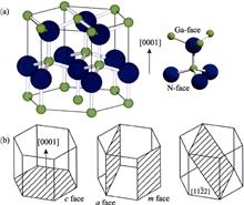
Sapphire possesses excellent hardness, strength, and UV-IR transmittance properties, which make it as an excellent candidate for IR window and transparent armor material. Sapphire plate with large size grown by the Edge-defined Film-fed Growth (EFG) method appears “near-net” size, which can minimize processing cost. Recently Nanjing Tongli Crystal Material Institute Co., Ltd. has accomplished large size sapphire plate successfully by EFG method, with size up to 415 mm × 810 mm × 12 mm.
Jan. 17, 2023Vol. 38 Issue 3 363 (2023)
© Copyright 2018-2021 | Chinese Laser Press.
All Rights Reserved 沪ICP备15018463号-20