


Please enter the answer below before you can view the full text.


2023
Volume: 49 Issue 6
9 Article(s)

Xinquan ZHANG, Xi XIAO, and Shaohua YU
Microelectronics technology has enabled electronic devices from discrete to integrated, bringing exponential improvements in cost, reliability, power consumption, volume and other aspects for decades, which is the key to the wide application of electronic information technology. Currently, electronic information technology is facing bottlenecks such as bandwidth and energy consumption, and Moore’s Law is struggling. As another major carrier of information, photons have characteristics such as high bandwidth, high speed, low power consumption, and high parallelism. The continued progress of information technology must rely more on photons. However, the cost, reliability, and scale productivity of photonic devices lag behind the electronic devices. Therefore, based on the historical experience of the development of electronic devices, we propose the " microelectronization" of optoelectronics, emphasizing that optoelectronics take " integration" as the development track and " photoelectric fusion" as the development direction.Taking integration as the development track is to emphasize that optoelectronics should learn from microelectronics in order to meet the requirements of modern information systems for devices. The integrated development of optoelectronics has three main characteristics: the chip platform basing on silicon; the steady increase in integration scale; and the evolution of production mode towards fabless.Taking photoelectric integration as the development direction, it emphasizes the necessity of the combination of optoelectronics and microelectronics, and jointly solve the challenges of bandwidth, rate, power consumption and other challenges currently faced by information technology through device integration and function integration of the two, so as to meet the requirements of digital twins, metaverse and other applications. Photoelectronic fusion mainly has two levels: chip and system, involving monolithic optoelectronic integration, Co Packaged Optics (CPO), hybrid optoelectronic integration, device disaggregation, photoelectric hybrid computing, etc.The " microelectronization" of optoelectronics is not only a technological development guide, but also will have a significant impact on the information optoelectronics industry. The article have conducted open-minded thinking from the perspectives of market, competition, enterprises, products, etc., and pointed out that it may lead to industry reshaping.The " microelectronization" of the development of information optoelectronics is an objective requirement for the continued advancement of information technology. On the one hand, photons are being generalized from transmission technology to ubiquitous connection technology in the entire Information Communications Technology (ICT) domain, from the ground to the ocean and space at the macroscale, and from the shelf and board to the package, and chip at the microscale. On the other hand, photons will be generalized from bandwidth providing technology to a basic hardware technology for the entire ICT domain, from transmission and connection to complex functional domains such as computation, processing, and routing. The " microelectronization" of optoelectronics will enable photons not only have the potential but also the ability to fully utilize their advantages to support the continued progress of the information technology.
Dec. 10, 2023Vol. 49 Issue 6 1 (2023)
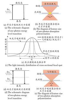
Mian WU, Lin WU, and Jin TAO
Metasurface is a thin layer that composed of periodic subwavelength artificial structures. By vibrating together with the incident electromagnetic waves, it introduces the phase jump, which breaks the traditional dependence on spatial optical path accumulation and exhibits unique electromagnetic characteristics. Metasurface has attracted great interest during the past ten years due to its ultra-thin thickness, ultrashort modulation distance and manipulation of light with ultrahigh resolution, superior to traditional optical elements. As the two-dimensional counterpart of metamaterials, it is easier to manufacture and integrate into the devices with operating wavelength ranging from microwaves to visible. The manufacturing processes commonly used for metasurfaces include ultraviolet lithography, electron beam lithography, focused ion beam lithography and nanoimprinting. However, the mass application still faces contradictions between processing accuracy and mass manufacturing and processing costs. Two-photon 3-Dimensional (3D) printing technology which is based on femtosecond pulse laser and two-photon polymerization reaction can fabricate metasurface with high precision and complex 3D structure by only one-step lithography without mask. It has the merits of processing convenience and flexibility, and has the potential of large-scale manufacturing. Therefore, it is widely used in the study and fabrication of metasurface. The paper reviews recent researches on metasurface optical devices fabricated by two-photon 3D printing technologies. An introduction to the concept, advantages and processing methods of metasurface is presented firstly, followed by the principle, development, and technological advantages of two-photon 3D printing. Recent study on metasurface devices ranging from plasmonic metasurfaces, metalens, metasurfaces for nano-display and holography, and metasurfaces integrated into fiber facet are reviewed respectively. Finally, the discussion and comments on metasurface devices based on two-photon 3D printing are given.
Dec. 10, 2023Vol. 49 Issue 6 11 (2023)
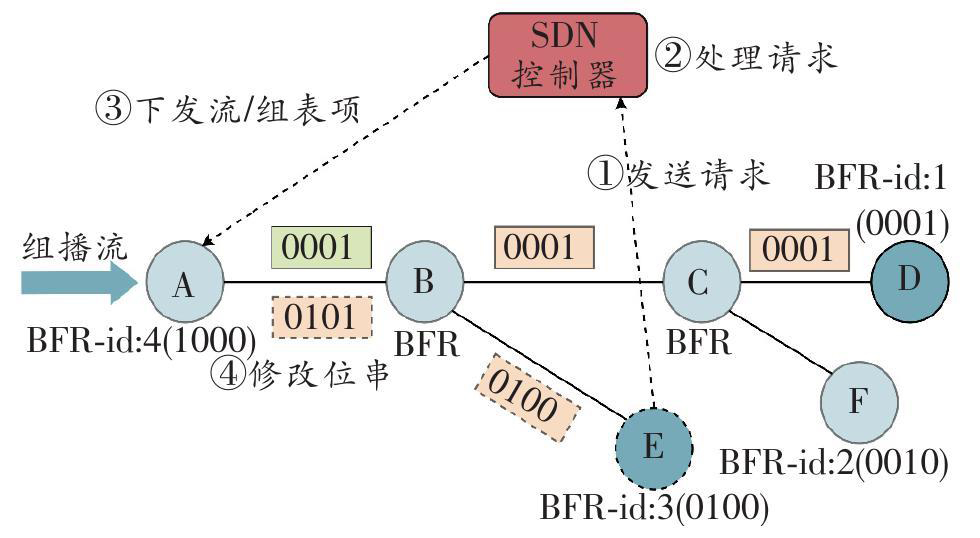
Qian DAI, Yanping LIU, Ximin YANG, and Wan TANG
【Objective】Aiming at the problem that BitString can not represent all Bit-Forwarding Routers (BFRs) in large-scale Software Defined Networking (SDN) multicast based on Bit Index Explicit Replication (BIER) due to the limited length, this study designs a Hierarchical Domain (HD)-BIER model and devises its construction algorithm.【Methods】The HD-BIER model is a multi-layer BIER network composed of multiple small-scale Sub Domains (SD), which enables BIER to support a number of devices exceeding the capacity of the BitString representation in large-scale networks. The proposed HD-BIER construction algorithm takes into account the BitString Length (BSL) limitation, link lengths between nodes, and network connectivity. It leverages the concept of community partition algorithms and introduces a modularity function based on node similarity as an evaluation metric for BIER SD partitioning. The construction follows a bottom-up approach to dynamically build the HD-BIER network.【Results】The simulation results show that the HD-BIER construction algorithm can effectively construct HD-BIER networks that exceed the BSL limit in either simple networks or the complex networks with a large number of nodes. Additionally, the resulting HD-BIER model not only ensures normal transmission of multicast service data flows through the gradual encapsulation and decapsulation of BitString layers but also maintains SDN multicast communication performance throughout this process.【Conclusion】The simulation results validate that the proposed HD-BIER model presents an effective multicast service support solution for even larger-scale networks.
Dec. 10, 2023Vol. 49 Issue 6 32 (2023)
Wenhui LI, Shifeng XIA, Tao WEI, and Meichun WANG
【Objective】Optical Cross Connect (OXC) technology has solved some problems of insufficient electric crossover capacity of Optical Transport Network (OTN) system, as well as complex manual fiber connection and inflexible scheduling between Fixed Optical Add/Drop Multiplexer (FOADM)/Reconfigurable Optical Add/Drop Multiplexer (ROADM) boards. This paper studies how to introduce OXC technology into OTN Metropolitan Area Network (MAN) to improve the flexibility of the network and solve some network security problems caused by the over concentration of OXC.【Methods】This paper introduces the advantages of OXC technology, and summarizes the architecture of the OTN system in the existing network, as well as the security configuration mode of the bearer service. By establishing various OXC application models, the paper compares and analyzes the flexibility and security of various models.【Results】After testing in the existing network, the paper summarizes various model evaluation indicators, and finds the optimal application scheme.【Conclusion】In this paper, an all-optical MAN construction model based on OXC is innovatively proposed to promote the application and development of OXC technology, strengthen the scheduling capability between computing forces, and form a new infrastructure of computing network integration. It finally provides users with low latency, highly reliable, end-to-end computing connections.
Dec. 10, 2023Vol. 49 Issue 6 40 (2023)
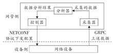
Xu ZHANG, Qinglin DENG, Peng CHEN, and Yunhao Li
【Objective】The scale of Software Defined Network (SDN) equipment is increasing, and more services are carried. Aiming at the problem that the traditional Optical Transport Network (OTN) devices cannot meet the requirements of large-scale and high-performance network management by using Simple Network Manager Protocol (SNMP) to collect performance data, this paper proposes an OTN device performance acquisition system based on Telemetry architecture.【Methods】By designing a distributed data model conversion and data coding architecture, the efficiency of data conversion and coding and the scale of the acquisition system are improved. At the same time, the computing power of the equipment is balanced. The equipment regularly collects and reports performance data to the collector in seconds.【Results】This paper compares and analyzes the performance collection capability of the device using SNMP and the device deploying Telemetry.【Conclusion】The results show that the system has more advantages in data model conversion and coding, data transmission efficiency, timeliness of data acquisition and flexibility of data acquisition, which may meet the requirements of SDN for intelligent operation and maintenance.
Dec. 10, 2023Vol. 49 Issue 6 45 (2023)
Jian LAN, Haiyang WU, Xiangdong CHEN, Shaoqing ZHOU, and Yabo HOU
【Objective】Focusing on the strategic goal of building an internationally leading energy Internet enterprise with Chinese characteristics, in accordance with the promotion of the deep integration and application of advanced information and communication technologies and advanced energy technologies, and focusing on the overall requirements of improving the power communication network to support and guarantee the safe operation of the power grid, Suzhou Electric Power launched the construction of a 220 kV protection private communication network since 2019. There exist problems with the 220 kV relay protection channel in Suzhou, such as long repair time, high occupancy of communication cabinet resources, and mixed networking of protection and communication services, which pose hidden dangers to the safe operation of the power grid.【Methods】This paper analyzes the current status and existing problems of Suzhou 220 kV relay protection channel. Combined with the actual situation of optical communication network in Suzhou, this paper proposes using 2 Mbit/s optical interface to directly connect protection equipment for carrying the relay protection channel of B port, and refines the power transformation plan, networking mode, protection business bearing mode, and network management bearing mode.【Results】Utilizing the respective characteristics of the direct channels with fiber optic and the multiplexing channels with protection private communication network, Suzhou Electric Power has built a protection private communication network which covers all transformer substations owning 220 kV outlets by customizing the small private communication transmission equipment that matches relay protection services.【Conclusion】The protection private communication network accessing to the centralized transmission equipment network management could monitor relay protection channels and achieve the observability and testability of the relay protection channels. It has advantages such as rapid failure positioning, failure isolation, and channel detour and comprehensively improves the reliability, independence, flexibility, and operation convenience of the relay protection channels. The protection private communication network has achieved significant application results and innovative results, which is also a beneficial exploration for the application of " 3 routes" for the protect channels.
Dec. 10, 2023Vol. 49 Issue 6 51 (2023)
Shaoheng LIN
【Objective】For the implementation of Trans Impedance Amplifier (TIA) in 400 Gbit/s Dual Polarization (DP)– 16 Quadrature Amplitude Modulation (QAM) coherent receiver.【Methods】A 64 GBaud dual channels differential linear TIA in advanced Silicon Germanium Bipolar Complementary Metal Oxide Semiconductor Heterojunction Bipolar Transistor (SiGe BiCMOS HBT) process is proposed. The chip consists of two identical signal amplifying paths for the I and Q signals of Coherent Receiver. The path utilities full differential shunt-shunt feedback structure as TIA stage, and consequent two Variable Gain Amplifier (VGA) stages in series to amplify further, and Current Mode Logic (CML) buffer with single-end 50 Ω output impedance as the output stage. The chip integrates two independent Direct Current Restore (DCR) loops to remove the input direct current component and direct current offset at the core output node, and integrates Direct Current Offset Cancellation (DCOC) loop to remove the output direct current offsets due to the differential pairs mismatch along the VGA and buffer stages. An Automatic Gain Control (AGC) loop is built in to adjust automatically the trans-impedance gain of TIA stage and gain of VGA stages based on input amplitude detecting, which is aimed to avoid saturation distortion. To optimize output impedance matching and reduce the impact of parasitic capacitance of Electrical Static Discharge (ESD) diodes, a three ports bridge-T network inductive peaking technique is inserted in the output node to optimize the output return loss and improve the bandwidth. The chip is designed and manufactured in advanced SiGe BiCMOS HBT process. The die size is 1.6 mm×1.8 mm, and the channel pitch is 625 μm. The chip is assembled with Photodiode (PD), junction capacitance Cpd=50 fF and other coherent optical components into Integrated Coherent Receiver (ICR) for testing.【Results】The test results show that, the differential gain is 5 kΩ, and the 3 dB bandwidth is 32 GHz. The Total Harmonic Distortion (THD) is less than 2%, and the overload optical input is 3 dBm. The chip is powered by a single 3.3 V supply, and the static power dissipation is only 250 mW.【Conclusion】The chip can be applied in 64 GBaud coherent receiver, and implement 400 Gbit/s per lambda transmission with DP-16QAM modulation.
Dec. 10, 2023Vol. 49 Issue 6 57 (2023)
Teng-xiao ZHANG, and Yang QIU
In recent years, with the continuous promotion of the " Ocean Power" strategy, Underwater Wireless Optical Communication (UWOC) has played an important role in marine military, underwater environment monitoring, submarine oil exploration and marine science research due to its advantages in large bandwidth, fast rate, low power consumption and high security. UWOC has become a new feasible underwater communication technology. The positioning technology is now regarded as the basis of UWOC applications and one of the key techniques in underwater target detection & moving object tracking, which has been favored by researchers. In this paper, the development of UWOC and related research results are introduced in detail, with diverse UWOC localization methods being analyzed. Besides, the research status, the challenges and the development prospects for UWOC localization technology are also discussed.
Dec. 10, 2023Vol. 49 Issue 6 64 (2023)
Yu-ze LI, and Xin-an LI
In the vehicle to infrastructure communication, the millimeter wave beam width is narrow and user equipment mobility is high. Therefore, effective millimeter wave beam selection is a key and challenging task. Aiming at the problem of high overhead in the beam search process, this paper proposes a millimeter-wave beam selection algorithm based on radar and location information. The proposed algorithm trains a neural network structure on the lidar and beam tracking channel datasets using the Top-k classification metric. It also predicts the best beam pair using the Global Context Net (GCNet) model. The simulation results show that the performance of the proposed algorithm is significantly improved in the classification and recognition accuracy. At the same time, it only needs to search 5 beams to approach the performance of the exhaustive search, which greatly reduces the beam search overhead.
Dec. 10, 2023Vol. 49 Issue 6 72 (2023)
© Copyright 2018-2021 | Chinese Laser Press.
All Rights Reserved 沪ICP备15018463号-20