


 View fulltext

2022
Volume: 5 Issue 9
4 Article(s)

Zhiqiang Yu, Nan Zhang, Jianxin Wang, Zijie Dai, Cheng Gong, Lie Lin, Lanjun Guo, and Weiwei Liu
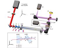
In this study, an optical setup for generating terahertz (THz) pulses through a two-color femtosecond laser filament was carefully designed to achieve a precise overlap of two-color laser pulses in space and time. β-barium borate (BBO), α-BBO, and a dual-wavelength plate were used to compensate the phase delay of the two-color lasers. Tilting of α-BBO could further realize the precise spatial overlap of the two beams by counteracting the walk-off effect. The maximum output THz pulse energy reached 21 μJ in argon gas when using a commercial Ti:sapphire laser with a pulse energy of 6 mJ at a 1 kHz repetition rate. The corresponding conversion efficiency exceeded 0.35%.In this study, an optical setup for generating terahertz (THz) pulses through a two-color femtosecond laser filament was carefully designed to achieve a precise overlap of two-color laser pulses in space and time. β-barium borate (BBO), α-BBO, and a dual-wavelength plate were used to compensate the phase delay of the two-color lasers. Tilting of α-BBO could further realize the precise spatial overlap of the two beams by counteracting the walk-off effect. The maximum output THz pulse energy reached 21 μJ in argon gas when using a commercial Ti:sapphire laser with a pulse energy of 6 mJ at a 1 kHz repetition rate. The corresponding conversion efficiency exceeded 0.35%.
Sep. 25, 2022Vol. 5 Issue 9 210065 (2022)
Caihong Li, Wen Du, Yixuan Huang, Jihua Zou, Lingzhi Luo, Song Sun, Alexander O. Govorov, Jiang Wu, Hongxing Xu, and Zhiming Wang
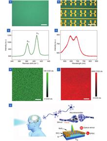
The human visual system, dependent on retinal cells, can be regarded as a complex combination of optical system and nervous system. Artificial retinal system could mimic the sensing and processing function of human eyes. Optically stimulated synaptic devices could serve as the building blocks for artificial retinas and subsequent information transmission system to brain. Herein, photonic synaptic transistors based on polycrystalline MoS2, which could simulate human visual perception and brain storage, are presented. Moreover, the photodetection range from visible light to near-infrared light of MoS2 multilayer could extend human eyes’ vision limitation to near-infrared light. Additionally, the photonic synaptic transistor shows an ultrafast speed within 5 μs and ultralow power consumption under optical stimuli about 40 aJ, several orders of magnitude lower than biological synapses (50 ms and 10 fJ). Furthermore, the backgate control could act as emotional modulation of the artificial brain to enhance or suppress memory function, i.e. the intensity of photoresponse. The proposed carrier trapping/detrapping as the main working mechanism is presented for the device. In addition, synaptic functionalities including short synaptic plasticity, long synaptic plasticity and paired-pulse facilitation could be successfully simulated based on the prepared device. Furthermore, the large difference between short synaptic plasticity and long synaptic plasticity reveals the better image pre-processing function of the prepared photonic synapses. The classical Pavlovian conditioning associated with the associative learning is successfully implemented as well. Therefore, the efficient and rich functionalities demonstrate the potential of the MoS2 synaptic device that integrates sensing-memory-preprocessing capabilities for realizing artificial neural networks with different emotions that mimic human retina and brain.The human visual system, dependent on retinal cells, can be regarded as a complex combination of optical system and nervous system. Artificial retinal system could mimic the sensing and processing function of human eyes. Optically stimulated synaptic devices could serve as the building blocks for artificial retinas and subsequent information transmission system to brain. Herein, photonic synaptic transistors based on polycrystalline MoS2, which could simulate human visual perception and brain storage, are presented. Moreover, the photodetection range from visible light to near-infrared light of MoS2 multilayer could extend human eyes’ vision limitation to near-infrared light. Additionally, the photonic synaptic transistor shows an ultrafast speed within 5 μs and ultralow power consumption under optical stimuli about 40 aJ, several orders of magnitude lower than biological synapses (50 ms and 10 fJ). Furthermore, the backgate control could act as emotional modulation of the artificial brain to enhance or suppress memory function, i.e. the intensity of photoresponse. The proposed carrier trapping/detrapping as the main working mechanism is presented for the device. In addition, synaptic functionalities including short synaptic plasticity, long synaptic plasticity and paired-pulse facilitation could be successfully simulated based on the prepared device. Furthermore, the large difference between short synaptic plasticity and long synaptic plasticity reveals the better image pre-processing function of the prepared photonic synapses. The classical Pavlovian conditioning associated with the associative learning is successfully implemented as well. Therefore, the efficient and rich functionalities demonstrate the potential of the MoS2 synaptic device that integrates sensing-memory-preprocessing capabilities for realizing artificial neural networks with different emotions that mimic human retina and brain.
Sep. 25, 2022Vol. 5 Issue 9 210069 (2022)
Jovan Maksimovic, Jingwen Hu, Soon Hock Ng, Tomas Katkus, Gediminas Seniutinas, Tatiana Pinedo Rivera, Michael Stuiber, Yoshiaki Nishijima, Sajeev John, and Saulius Juodkazis
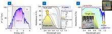
Light trapping photonic crystal (PhC) patterns on the surface of Si solar cells provides a novel opportunity to approach the theoretical efficiency limit of 32.3%, for light-to-electrical power conversion with a single junction cell. This is beyond the efficiency limit implied by the Lambertian limit of ray trapping ~ 29%. The interference and slow light effects are harnessed for collecting light even at the long wavelengths near the Si band-gap. We compare two different methods for surface patterning, that can be extended to large area surface patterning: 1) laser direct write and 2) step-&-repeat 5× reduction projection lithography. Large area throughput limitations of these methods are compared with the established electron beam lithography (EBL) route, which is conventionally utilised but much slower than the presented methods. Spectral characterisation of the PhC light trapping is compared for samples fabricated by different methods. Reflectance of Si etched via laser patterned mask was ~ 7% at visible wavelengths and was comparable with Si patterned via EBL made mask. The later pattern showed a stronger absorbance than the Lambertian limit6.Light trapping photonic crystal (PhC) patterns on the surface of Si solar cells provides a novel opportunity to approach the theoretical efficiency limit of 32.3%, for light-to-electrical power conversion with a single junction cell. This is beyond the efficiency limit implied by the Lambertian limit of ray trapping ~ 29%. The interference and slow light effects are harnessed for collecting light even at the long wavelengths near the Si band-gap. We compare two different methods for surface patterning, that can be extended to large area surface patterning: 1) laser direct write and 2) step-&-repeat 5× reduction projection lithography. Large area throughput limitations of these methods are compared with the established electron beam lithography (EBL) route, which is conventionally utilised but much slower than the presented methods. Spectral characterisation of the PhC light trapping is compared for samples fabricated by different methods. Reflectance of Si etched via laser patterned mask was ~ 7% at visible wavelengths and was comparable with Si patterned via EBL made mask. The later pattern showed a stronger absorbance than the Lambertian limit6.
Sep. 25, 2022Vol. 5 Issue 9 210086 (2022)
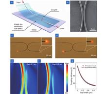
Wen Yu, Ni Yao, Jing Pan, Wei Fang, Xiong Li, Limin Tong, and Lei Zhang
Flexible strain sensors play an important role in electronic skins, wearable medical devices, and advanced robots. Herein, a highly sensitive and fast response optical strain sensor with two evanescently coupled optical micro/nanofibers (MNFs) embedded in a polydimethylsiloxane (PDMS) film is proposed. The strain sensor exhibits a gauge factor as high as 64.5 for strain ≤ 0.5% and a strain resolution of 0.0012% which corresponds to elongation of 120 nm on a 1 cm long device. As a proof-of-concept, highly sensitive fingertip pulse measurement is realized. The properties of fast temporal frequency response up to 30 kHz and a pressure sensitivity of 102 kPa?1 enable the sensor for sound detection. Such versatile sensor could be of great use in physiological signal monitoring, voice recognition and micro-displacement detection.Flexible strain sensors play an important role in electronic skins, wearable medical devices, and advanced robots. Herein, a highly sensitive and fast response optical strain sensor with two evanescently coupled optical micro/nanofibers (MNFs) embedded in a polydimethylsiloxane (PDMS) film is proposed. The strain sensor exhibits a gauge factor as high as 64.5 for strain ≤ 0.5% and a strain resolution of 0.0012% which corresponds to elongation of 120 nm on a 1 cm long device. As a proof-of-concept, highly sensitive fingertip pulse measurement is realized. The properties of fast temporal frequency response up to 30 kHz and a pressure sensitivity of 102 kPa?1 enable the sensor for sound detection. Such versatile sensor could be of great use in physiological signal monitoring, voice recognition and micro-displacement detection.
Sep. 25, 2022Vol. 5 Issue 9 210101 (2022)
© Copyright 2018-2021 | Chinese Laser Press.
All Rights Reserved 沪ICP备15018463号-20