


 View fulltext

2022
Volume: 5 Issue 6
5 Article(s)

Liuyang Yang, Yanpeng Li, Fang Fang, Liangye Li, Zhijun Yan, Lin Zhang, and Qizhen Sun
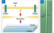
A microfiber with large evanescent field encapsulated in PDMS is proposed and demonstrated for ultrasound sensing. The compact size and large evanescent field of microfiber provide an excellent platform for the interaction between optical signal and ultrasound wave, exhibiting a high sensitivity of 3.5 mV/kPa, which is approximately 10 times higher than the single-mode fiber sensor. Meanwhile, a phase feedback stabilization module is introduced into the coherent demodulation system for long-term stable measurement. In addition, a photoacoustic tomography experiment with the microfiber ultrasound sensor is implemented to verify the excellent performance on imaging, with the depth of 12 mm, the highest lateral resolution of 65 μm and axial resolution of 250 μm, respectively. The highly sensitive microfiber ultrasound sensor provides a competitive alternative for various applications, such as industrial non-destructive testing, biomedical ultrasound and photoacoustic imaging.A microfiber with large evanescent field encapsulated in PDMS is proposed and demonstrated for ultrasound sensing. The compact size and large evanescent field of microfiber provide an excellent platform for the interaction between optical signal and ultrasound wave, exhibiting a high sensitivity of 3.5 mV/kPa, which is approximately 10 times higher than the single-mode fiber sensor. Meanwhile, a phase feedback stabilization module is introduced into the coherent demodulation system for long-term stable measurement. In addition, a photoacoustic tomography experiment with the microfiber ultrasound sensor is implemented to verify the excellent performance on imaging, with the depth of 12 mm, the highest lateral resolution of 65 μm and axial resolution of 250 μm, respectively. The highly sensitive microfiber ultrasound sensor provides a competitive alternative for various applications, such as industrial non-destructive testing, biomedical ultrasound and photoacoustic imaging.
Jun. 25, 2022Vol. 5 Issue 6 200076 (2022)
Long Wen, Xianghong Nan, Jiaxiang Li, David R. S. Cumming, Xin Hu, and Qin Chen
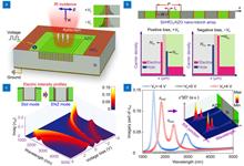
Epsilon-near-zero (ENZ) modes have attracted extensive interests due to its ultrasmall mode volume resulting in extremely strong light-matter interaction (LMI) for active optoelectronic devices. The ENZ modes can be electrically toggled between on and off states with a classic metal-insulator-semiconductor (MIS) configuration and therefore allow access to electro-absorption (E-A) modulation. Relying on the quantum confinement of charge-carriers in the doped semiconductor, the fundamental limitation of achieving high modulation efficiency with MIS junction is that only a nanometer-thin ENZ confinement layer can contribute to the strength of E-A. Further, for the ENZ based spatial light modulation, the requirement of resonant coupling inevitably leads to small absolute modulation depth and limited spectral bandwidth as restricted by the properties of the plasmonic or high-Q resonance systems. In this paper, we proposed and demonstrated a dual-ENZ mode scheme for spatial light modulation with a TCOs/dielectric/silicon nanotrench configuration for the first time. Such a SIS junction can build up two distinct ENZ layers arising from the induced charge-carriers of opposite polarities adjacent to both faces of the dielectric layer. The non-resonant and low-loss deep nanotrench framework allows the free space light to be modulated efficiently via interaction of dual ENZ modes in an elongated manner. Our theoretical and experimental studies reveal that the dual ENZ mode scheme in the SIS configuration leverages the large modulation depth, extended spectral bandwidth together with high speed switching, thus holding great promise for achieving electrically addressed spatial light modulation in near- to mid-infrared regions. Epsilon-near-zero (ENZ) modes have attracted extensive interests due to its ultrasmall mode volume resulting in extremely strong light-matter interaction (LMI) for active optoelectronic devices. The ENZ modes can be electrically toggled between on and off states with a classic metal-insulator-semiconductor (MIS) configuration and therefore allow access to electro-absorption (E-A) modulation. Relying on the quantum confinement of charge-carriers in the doped semiconductor, the fundamental limitation of achieving high modulation efficiency with MIS junction is that only a nanometer-thin ENZ confinement layer can contribute to the strength of E-A. Further, for the ENZ based spatial light modulation, the requirement of resonant coupling inevitably leads to small absolute modulation depth and limited spectral bandwidth as restricted by the properties of the plasmonic or high-Q resonance systems. In this paper, we proposed and demonstrated a dual-ENZ mode scheme for spatial light modulation with a TCOs/dielectric/silicon nanotrench configuration for the first time. Such a SIS junction can build up two distinct ENZ layers arising from the induced charge-carriers of opposite polarities adjacent to both faces of the dielectric layer. The non-resonant and low-loss deep nanotrench framework allows the free space light to be modulated efficiently via interaction of dual ENZ modes in an elongated manner. Our theoretical and experimental studies reveal that the dual ENZ mode scheme in the SIS configuration leverages the large modulation depth, extended spectral bandwidth together with high speed switching, thus holding great promise for achieving electrically addressed spatial light modulation in near- to mid-infrared regions.
Jun. 25, 2022Vol. 5 Issue 6 200093 (2022)
Sarah Dittrich, Maximilian Spellauge, Stephan Barcikowski, Heinz P. Huber, and Bilal Gökce
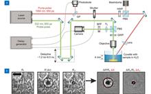
Laser ablation in liquid is a scalable nanoparticle production method with applications in areas like catalysis and biomedicine. Due to laser-liquid interactions, different energy dissipation channels such as absorption by the liquid and scattering at the ablation plume and cavitation bubble lead to reduced laser energy available for nanoparticle production. Ultrashort pulse durations cause unwanted nonlinear effects in the liquid, and for ns pulses, intra-pulse energy deposition attenuation effects are to be expected. However, intermediate pulse durations ranging from hundreds of picoseconds up to one nanosecond have rarely been studied in particular in single-pulse settings. In this study, we explore the pico- to nanosecond pulse duration regimes to find the pulse duration with the highest ablation efficiency. We find that pulse durations around 1–2 ns enable the most efficient laser ablation in liquid since the laser beam shielding by the ablation plume and cavitation bubble sets in only at longer pulse durations. Furthermore, pump-probe microscopy imaging reveals that the plume dynamics in liquids start to differ from plume dynamics in air at about 2 ns after pulse impact.Laser ablation in liquid is a scalable nanoparticle production method with applications in areas like catalysis and biomedicine. Due to laser-liquid interactions, different energy dissipation channels such as absorption by the liquid and scattering at the ablation plume and cavitation bubble lead to reduced laser energy available for nanoparticle production. Ultrashort pulse durations cause unwanted nonlinear effects in the liquid, and for ns pulses, intra-pulse energy deposition attenuation effects are to be expected. However, intermediate pulse durations ranging from hundreds of picoseconds up to one nanosecond have rarely been studied in particular in single-pulse settings. In this study, we explore the pico- to nanosecond pulse duration regimes to find the pulse duration with the highest ablation efficiency. We find that pulse durations around 1–2 ns enable the most efficient laser ablation in liquid since the laser beam shielding by the ablation plume and cavitation bubble sets in only at longer pulse durations. Furthermore, pump-probe microscopy imaging reveals that the plume dynamics in liquids start to differ from plume dynamics in air at about 2 ns after pulse impact.
Jun. 25, 2022Vol. 5 Issue 6 210053 (2022)
Xiao Yang, Yue Lin, Tingzhu Wu, Zijun Yan, Zhong Chen, Hao-Chung Kuo, and Rong Zhang
Augmented reality (AR) and virtual reality (VR) are two novel display technologies that are under updates. The essential feature of AR/VR is the full-color display that requires high pixel densities. To generate three-color pixels, the fluorescent color conversion layer inevitably includes green and red pixels. To fabricate such sort of display kits, inkjet printing is a promising way to position the color conversion layers. In this review article, the progress of AR/VR technologies is first reviewed, and in succession, the state of the art of inkjet printing, as well as two key issues — the optimization of ink and the reduction of coffee-ring effects, are introduced. Finally, some potential problems associated with the color converting layer are highlighted.Augmented reality (AR) and virtual reality (VR) are two novel display technologies that are under updates. The essential feature of AR/VR is the full-color display that requires high pixel densities. To generate three-color pixels, the fluorescent color conversion layer inevitably includes green and red pixels. To fabricate such sort of display kits, inkjet printing is a promising way to position the color conversion layers. In this review article, the progress of AR/VR technologies is first reviewed, and in succession, the state of the art of inkjet printing, as well as two key issues — the optimization of ink and the reduction of coffee-ring effects, are introduced. Finally, some potential problems associated with the color converting layer are highlighted.
Jun. 25, 2022Vol. 5 Issue 6 210123 (2022)

Wagner Tavares Buono, and Andrew Forbes
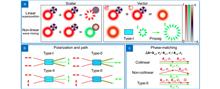
The interest in tailoring light in all its degrees of freedom is steadily gaining traction, driven by the tremendous developments in the toolkit for the creation, control and detection of what is now called structured light. Because the complexity of these optical fields is generally understood in terms of interference, the tools have historically been linear optical elements that create the desired superpositions. For this reason, despite the long and impressive history of nonlinear optics, only recently has the spatial structure of light in nonlinear processes come to the fore. In this review we provide a concise theoretical framework for understanding nonlinear optics in the context of structured light, offering an overview and perspective on the progress made, and the challenges that remain.The interest in tailoring light in all its degrees of freedom is steadily gaining traction, driven by the tremendous developments in the toolkit for the creation, control and detection of what is now called structured light. Because the complexity of these optical fields is generally understood in terms of interference, the tools have historically been linear optical elements that create the desired superpositions. For this reason, despite the long and impressive history of nonlinear optics, only recently has the spatial structure of light in nonlinear processes come to the fore. In this review we provide a concise theoretical framework for understanding nonlinear optics in the context of structured light, offering an overview and perspective on the progress made, and the challenges that remain.
Jun. 25, 2022Vol. 5 Issue 6 210174 (2022)
© Copyright 2018-2021 | Chinese Laser Press.
All Rights Reserved 沪ICP备15018463号-20