


 View fulltext

2020
Volume: 3 Issue 10
3 Article(s)

Kiyosh Asakawa, Yoshimasa Sugimoto, and Shigeru Nakamura
In recent decades, silicon photonics has attracted much attention in telecom and data-com areas. Constituted of high refractive-index contrast waveguides on silicon-on-insulator (SOI), a variety of integrated photonic passive and active devices have been implemented supported by excellent optical properties of silicon in the mid-infrared spectrum. The main advantage of the silicon photonics is the ability to use complementary metal oxide semiconductor (CMOS) process-compatible fabrication technologies, resulting in high-volume production at low cost. On the other hand, explosively growing traffic in the telecom, data center and high-performance computer demands the data flow to have high speed, wide bandwidth, low cost, and high energy-efficiency, as well as the photonics and electronics to be integrated for ultra-fast data transfer in networks. In practical applications, silicon photonics started with optical interconnect transceivers in the data-com first, and has been now extended to innovative applications such as multi-port optical switches in the telecom network node and integrated optical phased arrays (OPAs) in light detection and ranging (LiDAR). This paper overviews the progresses of silicon photonics from four points reflecting the recent advances mentioned above. CMOS-based silicon photonic platform technologies, applications to optical transceiver in the data-com network, applications to multi-port optical switches in the telecom network and applications to OPA in LiDAR system.
Oct. 28, 2020Vol. 3 Issue 10 200011-1 (2020)
Yuechen Jia, Shixiang Wang, and Feng Chen
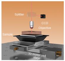
Optical waveguides are far more than mere connecting elements in integrated optical systems and circuits. Benefiting from their high optical confinement and miniaturized footprints, waveguide structures established based on crystalline materials, particularly, are opening exciting possibilities and opportunities in photonic chips by facilitating their on-chip integration with different functionalities and highly compact photonic circuits. Femtosecond-laser-direct writing (FsLDW), as a true three-dimensional (3D) micromachining and microfabrication technology, allows rapid prototyping of on-demand waveguide geometries inside transparent materials via localized material modification. The success of FsLDW lies not only in its unsurpassed aptitude for realizing 3D devices but also in its remarkable material-independence that enables cross-platform solutions. This review emphasizes FsLDW fabrication of waveguide structures with 3D layouts in dielectric crystals. Their functionalities as passive and active photonic devices are also demonstrated and discussed.
Oct. 23, 2020Vol. 3 Issue 10 190042-1 (2020)
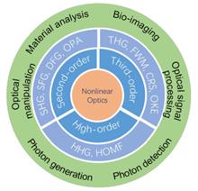
Silu Zhang, Liwei Liu, Sheng Ren, Zilin Li, Yihua Zhao, Zhigang Yang, Rui Hu, and Junle Qu
Nonlinear optics, which is a subject for studying the interaction between intense light and materials, has great impact on various research fields. Since many structures in biological tissues exhibit strong nonlinear optical effects, nonlinear optics has been widely applied in biomedical studies. Especially in the aspect of bio-imaging, nonlinear optical techniques can provide rapid, label-free and chemically specific imaging of biological samples, which enable the investigation of biological processes and analysis of samples beyond other microscopy techniques. In this review, we focus on the introduction of nonlinear optical processes and their applications in bio-imaging as well as the recent advances in this filed. Our perspective of this field is also presented.
Oct. 23, 2020Vol. 3 Issue 10 200003-1 (2020)
© Copyright 2018-2021 | Chinese Laser Press.
All Rights Reserved 沪ICP备15018463号-20