 View fulltext
The Institute of Optics and Electronics, Chinese Academy of Sciences is glad to announce the launch of a new free online journal Opto-Electronic Advances (OEA). Optics and opto-electronics are of paramount importance in the development of science and technology during the last four hundred years. With the emergence of new manufacturing and characterization technologies, these areas have developed into a new phase. At this stage, our existing journal Opto-electronic Engineering (OEE), which mainly reports the cutting-edge technical advances and engineering applications of optics and opto-electronics in China, could not meet the global technical developments and communications requirements of these areas. In order to promote international academic and technical communications, we are pleased to launch a new English journal ——OEA. It will be more aimed at theoretical and technological innovations covering all significant research activities in the broad area of optics and opto-electronics. The journal provides a chance for authors to publish the latest research results, and for readers to learn breakthroughs and advances more conveniently and efficiently.
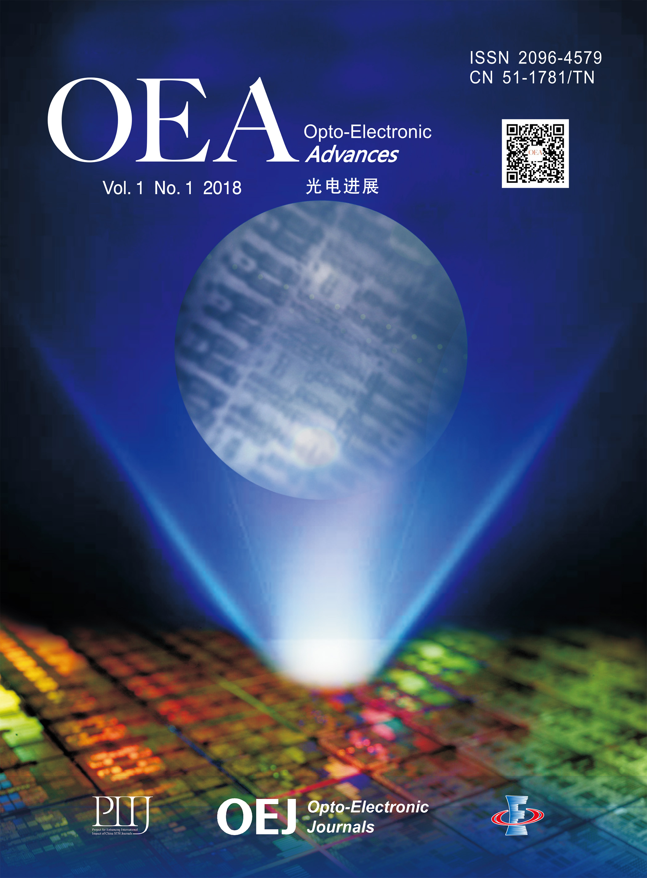
Optical microscope is one of the most popular characterization techniques for general purposes in many fields. It is distinguished from the vacuum or tip-based imaging techniques for its flexibility, low cost, and fast speed. However, its resolution limits the functionality of current optical imaging performance. While microspheres have been demonstrated for improving the observation power of optical microscope, they are directly deposited on the sample surface and thus the applications are greatly limited. We develop a remote-mode microsphere nano-imaging platform which can scan freely and in real-time across the sample surfaces. It greatly increases the observation power and successfully characterizes various practical samples with the smallest feature size down to 23 nm. This method offers many unique advantages, such as enabling the detection to be non-invasive, dynamic, real-time, and label-free, as well as leading to more functionalities in ambient air and liquid environments, which extends the nano-scale observation power to a broad scope in our life.
3D printing is disrupting the design and manufacture of electronic products. 3D printing electronics offers great potential to build complex object with multiple functionalities. Particularly, it has shown the unique ability to make embedded electronics, 3D structural electronics, conformal electronics, stretchable electronics, etc. 3D printing electronics has been considered as the next frontier in additive manufacturing and printed electronics. Over the past five years, a large number of studies and efforts regarding 3D printing electronics have been carried out by both academia and industries. In this paper, a comprehensive review of recent advances and significant achievements in 3D printing electronics is provided. Furthermore, the prospects, challenges and trends of 3D printing electronics are discussed. Finally, some promising solutions for producing electronics with 3D printing are presented.


