


 View fulltext
Yu-Fei QI, Wen-Juan WANG, Jing-Hua SUN, Wen WU, Yan LIANG, Hui-Dan QU, Min ZHOU, and Wei LU
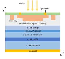
We described a high-performance planar InGaAsP/InP single-photon avalanche diode (SPAD) with a separate absorption, grading, charge and multiplication (SAGCM) heterostructure. By electric field regulation and defects control, the SPAD operated in the gated-mode at 293 K with a photon detection efficiency (PDE) of 70%, a dark count rate (DCR) of 14.93 kHz and an after-pulse probability (APP) of 0.89%. Furthermore, when operated in the active quenching mode with a dead time of 200 ns, a PDE of 12.49% and a DCR of 72.29 kHz were achieved at room temperature.
Feb. 25, 2024Vol. 43 Issue 1 1 (2024)
Jia-Ping SU, Xiao-Hao ZHOU, Zhou TANG, Liu-Yan FAN, Shun-Ji XIA, Ping-Ping CHEN, and Ze-Zhong CHEN
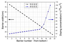
In this paper, the GaAs/AlGaAs non-uniform quantum well infrared detector material was successfully grown by molecular beam epitaxy (MBE), and the microstructure was characterized in detail. The performance difference between the non-uniform quantum well structure and the conventional quantum well infrared detector is analyzed and compared, and the performance change of the non-uniform quantum well infrared detector under different well widths is comparatively studied. The microstructure of non-uniform quantum well infrared detector materials was analyzed by high resolution transmission electron microscopy (HRTEM) combined with energy dispersive spectroscopy (EDS), and the non-uniform well doping was characterized by secondary ion mass spectrometry (SIMS). The results show that the crystal quality of the non-uniform quantum well epitaxial material is very good, and the non-uniform quantum well structure and doping concentration are also in good agreement with the design values. The unit quantum well infrared detector has been successfully fabricated. The research results show that for non-uniform quantum well infrared detectors, the electric field distribution of the quantum well can be changed by changing the doping concentration and barrier width of each well. Compared with traditional uniform quantum well infrared detectors, their dark current significantly decreases (by about an order of magnitude). Moreover, under different well widths, the transition modes of non-uniform quantum wells can change, and the devices with bound state to quasi-bound state transition modes (B-QB) have better blackbody response and lower dark current.
Feb. 25, 2024Vol. 43 Issue 1 7 (2024)
Miao He, Yi Zhou, Xiang-Xiao Ying, Zhao-Min Liang, Min Huang, Zhi-Fang Wang, Yi-Hong Zhu, Ke-Cai Liao, Nan Wang, and Jian-Xin Chen
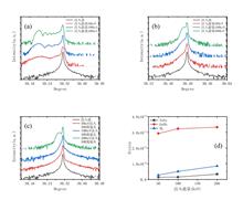
Class II superlattice infrared detectors generally detect infrared radiation through mesa junction, while transverse PN junction is realized through ion implantation. On the one hand, the material epitaxy process is simple, and at the same time, the advantages of superlattice material that the transverse diffusion length is far higher than the longitudinal can be used to improve the transport of photogenerated current carriers, and it is easy to make high-density planar arrays. In this paper, the effects of Si ion implantation with different energies and annealing on the properties of InAs/GaSb type II superlattice materials were studied by using a variety of material characterization techniques. Through Si ion implantation, the epitaxial material changes from P type to N type, and the vertical tensile strain is generated in the superlattice material. The lattice constant becomes larger, and the mismatch increases with the increase of implantation energy. The mismatch before implantation is -0.012%. When the implantation energy reaches 200 keV, the mismatch reaches 0.072%, and the superlattice partially relaxes, with the relaxation degree of 14%. After annealing at 300 ° C for 60 s, the superlattice returns to the fully strained state, and the lattice constant becomes smaller, This tensile strain is caused by the diffusion of Ga-In caused by annealing and lattice shrinkage caused by Si substitution.
Feb. 25, 2024Vol. 43 Issue 1 15 (2024)
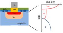
Jia-Mu LIN, Song-Min ZHOU, Xi WANG, Zhi-Kai GAN, Chun LIN, and Rui-Jun DING
An important branch of the three-generation infrared focal plane is high operating temperature (HOT) infrared detector. For HgCdTe n-on-p detectors, dark current can be suppressed with n+-n--p structure and good passivation, and then better performance of the detector will be obtained under high operating temperature. Based on the junction formation simulator, the junction formation parameters of HOT device are achieved and combined with the manufacture technology of optimized passivation layer, HgCdTe n-on-p infrared focal plane arrays which can operate at higher temperature was made in Shanghai Institute of Technical Physics(SITP). The performance of was studied at high operating temperature. One of mid-infrared detector has reached good performance under different operating temperature. The NETD is 6.10mK and operability is 99.96% at 80K, and the NETD is 11.0mK and operability is 99.50% at 150K , which reached the theoretical limit.
Feb. 25, 2024Vol. 43 Issue 1 23 (2024)
Chen-Wei ZHU, Xin-Yang LIU, Yan WU, Xin-Rong ZUO, Liu-Yan FAN, Ping-Ping CHEN, and Xiao-Mei QIN
CdTe(211)thin films are grown on GaAs(211)B substrates by molecular beam epitaxy(MBE), the influence of different process conditions on the surface morphology and optical properties of the CdTe epitaxial films are stematically studied. The study shows that under certain growth temperatures, growing CdTe thin films in a Te atmosphere and increasing the CdTe and Te beam ratio can significantly reduce the size and density of pyramid defects on the CdTe surface. When the CdTe and Te beam ratio is 6.5, the pyramid defects almost disappear, and the surface smoothness of the material is significantly improved. X-ray diffraction(XRD)also shows that the crystal quality of CdTe has significantly improved. Further Raman spectroscopy shows that with the increase of the CdTe and Te beam ratio, the A1 peak of Te weakens, and the intensity ratio of the CdTe LO and TO phonon peaks increases. Low-temperature photoluminescence(PL)studies also show that with the increase of the CdTe and Te beam ratio, the reduction of Cd vacancies can reduce the peak intensity of the deep energy level region related to impurity energy levels, while the half-width of the free exciton peak related to crystal quality reduces, and the optical quality of the material is significantly improved. This study explores the ideal process window and related mechanisms of CdTe/GaAs epitaxial materials, and provides a foundation for further epitaxial high-quality HgCdTe materials using this as a buffer layer.
Feb. 25, 2024Vol. 43 Issue 1 29 (2024)
Bi-Song TAN, Jian-Hong MAO, Shu-Xuan CHEN, Wei-Wei LI, Shi-Rui CHEN, Tian-Qing CHEN, Yu DU, Chen-Pan PENG, Xiong XIONG, Yong-Qiang ZHOU, Bo YU, and Shu WANG
In this paper, an investigation into the preparation technology and performance of 1280×1024 middle-wavelength (MW) HgCdTe infrared focal plane arrays (IRFPAs) with a pixel size of 10μm was introduced. The manufacturing process of these high-resolution FPAs involved the utilization of B+ injection to establish small-sized n-on-p junctions and the application of high-precision In-bump interconnection. Through development of the process, the adverse effects of the mismatch between HgCdTe devices and readout integrated circuits (ROICs) were mitigated, thereby reducing the likelihood of device failure. The assembled FPAs were evaluated to photoelectric performance evaluation at a temperature of 85 K. The experimental results demonstrate that the detector's spectral response encompasses a wavelength range of 3.67 μm to 4.88 μm. The highest pixel operability of the assembly can reach 99.95%. The average values of the noise equivalent temperature difference (NETD) and the dark current density for all the pixels of the assembly are respectively less than 16 mK and 2.1×10⁻⁸A/cm2. In comparison with a 15 μm pitch detector, the utilization of the 1280×1024 10 μm MWIR detector facilitated the capture of finer details in target images and extended the identification range. At present, this technology has been successfully transferred to the HgCdTe FPA production line of Zhejiang Juexin Microelectronics Co. Ltd. (ZJM). The production capacity and yield are constantly increasing.
Feb. 25, 2024Vol. 43 Issue 1 36 (2024)

Jing-Hua SUN, Wen-Juan WANG, Yi-Cheng ZHU, Zi-Lu GUO, Yu-Fei QI, and Wei-Ming XU
InGaAsP/InP single-photon avalanche diodes (SPADs) were gamma-irradiated with total doses of 10 krad (Si) and 20 krad (Si) and tested in situ and shift methods. After irradiation, the dark currents and dark count rates were degraded slightly, whereas the photon detection efficiency and the after pulse probability were basically unchanged. After a certain period of annealing at room temperature, these degradations were essentially recovered, indicating that transient ionization damage dominated in the gamma irradiation of InGaAsP/InP single-photon avalanche diodes.
Feb. 25, 2024Vol. 43 Issue 1 44 (2024)
Yu-Ran ZHEN, Jie DENG, Yong-Hao BU, Xu DAI, Yu YU, Meng-Die SHI, Ruo-Wen WANG, Tao YE, Gang CHEN, and Jing ZHOU
Polarization is an intrinsic degree of freedom of light. The detection of polarization light provides more information in addition to light intensity and wavelength. Infrared polarization detectors play a vital role in numerous applications, such as imaging, communication, remote sensing, and cosmology. However, traditional polarization detection systems are bulky and complex, hindering the miniaturization and integration of polarization detection. Recently, the development of on-chip infrared polarization detectors has become an area of great interest. In this review, we focus on two recent advanced research areas of on-chip infrared polarization detectors: polarization-sensitive materials and integration of polarization-selective optical coupling structures. We discuss the current research status, future challenges and opportunities for the development of on-chip infrared polarization detectors.
Feb. 25, 2024Vol. 43 Issue 1 52 (2024)
Zi-Lu GUO, Wen-Juan WANG, Hui-Dan QU, Liu--Yan FAN, Yi-Cheng ZHU, Ya-Jie WANG, Chang-Lin ZHENG, Xing-Jun WANG, Ping-Ping CHEN, and Wei LU
InP-based InGaAs/InP avalanche photodiodes (APDs) have high sensitivity to near-infrared light, making them ideal optoelectronic devices for weak signal and single-photon detection. However, as device structures become complex and advanced, with thickness and sizes ranging from quantum dots to several micrometers, performance is increasingly constrained by defects in the lattice of the material and the process conditions. Solid source molecular beam epitaxy (MBE) technology was used to deoxidize InP substrates under the atmosphere As and P, respectively, and epitaxially grow lattice-matched In0.53Ga0.47As film and InGaAs/InP avalanche APD full-structure materials. The experiment results demonstrate that As deoxidation has a distinct advantage over P deoxygenation in terms of MBE material quality, which can make a straight and sharp heterojunction interface, lower carrier concentrations, higher Hall mobilities, longer minority carrier lifetimes, and achieve suppression of dark current caused by point defects or impurity defects in the device. Therefore, As deoxidation can be applied effectively to enhance the quality of MBE materials. This work optimizes InP substrate InGaAs/InP epitaxial growth parameters and device fabrication conditions.
Feb. 25, 2024Vol. 43 Issue 1 63 (2024)
Xue BAI, Zi-Yu ZHANG, Lei-Jun XU, Xin-Ke ZHAO, and Xiao-Long FAN
This paper presents an improved 0.18 μm CMOS detector linear array with high voltage responsiveness. Each pixel consists of high-gain on-chip antenna, high-coupling self-mixing power detection circuit and integrated voltage amplifier. The differential detection circuit uses the cross-coupling capacitance of the source differential driven FET, coupling the terahertz differential signal to the gate and the source of the FET, and enhancing the strength of the self-mixing terahertz signal in the channel to achieve high responsiveness. Additionally, the detector is equipped with a high-gain differential annular antenna and an integrated voltage amplifier, which can effectively amplify the mixing signals, thus improving the signal-to-noise ratio of the system, and ultimately enhancing the detector‘s responsiveness. The 1 × 3 detector linear array system composed of three pixels makes full use of the characteristics of the multi-layer structure of CMOS. The voltage amplifier is arranged below the antenna ground plane, which improves the utilization of the chip area and effectively reduces the production cost. The area of the detector system is 0.5 mm2. When the gate is biased at 0.42 V, the measurement results show that, the maximum voltage responsiveness (Rv) can reach 43.8 kV /W under the radiation of 0.3 THz signal, and the corresponding minimum noise equivalent power (NEP) is 20.5 pW/Hz1/2. The dynamic measurement results show that the detector can distinguish different material blocks.
Feb. 25, 2024Vol. 43 Issue 1 70 (2024)
Kun HUANG, Hao YANG, Ruo-Xue LI, Ren ZHOU, Jun JIANG, Yue HE, and Yao-Ling TIAN
A 215~230 GHz Schottky varactor-based frequency doubler utilizing novel four-port balanced configuration has been developed with improved conversion efficiency and power-handling capability. The proposed doubler, featuring doubled number of anodes in conventional balanced ones, could inhibit the odd- and fourth-order harmonics. Thus, better conversion efficiency and doubled power handling capability could be achieved. At room temperature, the fabricated doubler exhibits a ~39.5% peak conversion efficiency (@218 GHz) for an input power of 196~340 mW, which is proved to be a perfect solution for the generation of high power terahertz waves even at higher frequencies.
Feb. 25, 2024Vol. 43 Issue 1 79 (2024)
Zhi-Chun LI, Yuan-Ting LYU, Ao ZHANG, and Jian-Jun GAO
An improved method for determination of extrinsic resistances for 70 nm InP high electron mobility transistor (HEMT) is proposed in this paper. A set of expressions have been derived from the equivalent circuit model under operating bias points (Vgs > Vth, Vds = 0 V). The extrinsic resistances are iterative determined using the discrepancy between simulated and measured S-parameters as an optimization criterion using the semi-analytical method. Good agreement between simulated and measured S-parameters under multi bias over the frequency range up to 110 GHz verifies the effectiveness of this extraction method.
Feb. 25, 2024Vol. 43 Issue 1 85 (2024)
Xiao-Kun WANG, Meng-Chao GUO, Lei-Lei LIANG, Wei LI, Dong-Ming TANG, Bao-Shan ZHANG, Jian-Dong YE, and Yi YANG
We synthesized C/Co composites via a facile one-step pyrolysis procedure and observed excellent dielectric dispersion properties at a 35 wt% filling concentration. At a thickness of 2.5 mm, the composites exhibited a minimum reflection of -23.7 dB at 11.2 GHz, with a bandwidth of 3.8 GHz (RL≤-10 dB). To further improve their absorption performance, we optimized the macrostructure of the absorber using an all-dielectric metamaterial design. The optimized design successfully extended the less than -10 dB absorption bandwidth to 15 GHz (7.0~22.0 GHz). Our results provide a useful reference for optimizing the preparation technology and structural design of high-performance microwave absorbers.
Feb. 25, 2024Vol. 43 Issue 1 91 (2024)
Shuo HUANG, Ming-Jian GU, Yong HU, Tian-Hang YANG, Chun-Yuan SHAO, and Chun-Ming ZHANG
The Infrared Hyperspectral Atmospheric Sounder II (HIRAS-II) mounted on Funyun-3E satellite (FY-3E) can realize vertical atmospheric detection, featuring hyper spectral, high sensitivity and high precision. When the satellite has been on-orbit, nonlinear response would occur due to instrument attenuation and environmental change, which affects the accuracy of on-orbit calibration. For nonlinear response problems, a nonlinear correction method based on in-band spectrum is proposed. Firstly, the nonlinear correction coefficient was solved based on the nonlinear characteristics of the out-of-band in low-frequency spectra, and the coefficient was input into the radiological calibration model as the initial value. The deviation between the black-body spectrum measured on board and the ideal spectrum was taken as the objective function, and the nonlinear correction coefficient was optimized by iterative calculation. Radiation calibration experiments have shown that the brightness temperature deviation of black body is reduced compared to uncorrected result and the out-of-band correction method using the proposed method.Based on the simultaneous nadir overpass method, After matching the observed data of HIRAS-II with IASI and calculating the mean brightness temperature deviation and the absolute value of the deviation, the mean brightness temperature deviation after nonlinear correction by the in-band correction method is -0.13K, which is better than the out-of-band correction method.
Feb. 25, 2024Vol. 43 Issue 1 98 (2024)
Ning LI, Yi-Fang GUO, Ji-Chao JIAO, Min PANG, and Wei XU
The detection of infrared small targets has been a challenging task in the field of computer vision due to the low percentage of small targets in the whole image and the presence of a large amount of clutter around the targets. We propose an algorithm based on associated directional gradient and mean contrast. The algorithm consists of two modules: the associated directional gradient module uses a Gaussian distribution model of infrared small targets, and adds the gradient in a single direction with the gradient in an adjacent direction to form a new feature called associated directional gradient, which enhances the real target, suppresses background clutter, and eliminates the effect of highlighting edges on the target detection. The mean contrast module incorporates directional information to calculate multi-directional contrast of the target. The minimum value of multi-directional contrast is chosen to suppress structural noise, and the idea of mean filtering is introduced into the calculation of contrast to suppress isolated noise in the background and further reduce the false alarm rate of detection. Experimental results on actual infrared images show that the algorithm can achieve better results in enhancing the signal-to-noise ratio of the target and suppressing the background noise.
Feb. 25, 2024Vol. 43 Issue 1 106 (2024)
Xu-Dong LAI, Wei-Ran PIAN, Li-Ming BO, and Li-Hua He
This paper proposes a method for extracting building LiDAR point cloud and orthophoto fusion based on improved genetic algorithm (IGA) for fine-grained 3D building modeling: The features based on point cloud and image are calculated and extracted to expand the feature space of point cloud; then, by using the improved genetic algorithm, the point cloud features are selected, construct and optimize feature space; finally, SVM classifier is used to achieve accurate extraction of building point cloud. The experimental results on ISPRS open data set Vaihingen test data show that the method proposed in this paper has high accuracy in building extraction. The experimental results on actual production data show that the building extraction accuracy is high and stable, which proves the advancement and universality of this method.
Feb. 25, 2024Vol. 43 Issue 1 116 (2024)
Ke-Wu LI, Shuang WANG, Meng-Wei LI, and Zhi-Bin WANG
In order to achieve the stress defect detection of infrared materials such as Si, Ge, and GaAs, two Photoelastic modulators working at different frequencies are cascaded to form a polarimetry system. The birefringence retardation and fast axis azimuth introduced by the stress defect are loaded into the modulation signals of the polarimetry system. The amplitudes of the fundamental and differential frequency terms were simultaneously obtained by using digital phase-locked technology, and then the two stress parameters are solved. A detailed analysis of the detection principle was conducted and an experimental system was established for verification. The experimental results show that this method has achieved stress defect detection with a standard deviation of 0.31 ° for stress direction angle and 0.72 nm for stress birefringence retardation. The high-speed, high-precision, and high repeatability stress defect detection are realized, and the measurement of stress defect distribution in a Ge samples are demonstrated. An effective method for infrared material quality testing, analysis, and evaluation is proposed.
Feb. 25, 2024Vol. 43 Issue 1 126 (2024)
Wang HOU, Ye-Pin QU, Jian-Qiang LIU, and Yu-Hai LYU
In response to the special situation where the near-infrared monocular vision pose measurement system in complex application environments deviates from the preset cooperative target object and cannot complete pose measurement, a monocular vision measurement method based on the random rough surface image around the cooperative target is proposed, as well as a dynamic self-healing method after image damage. By matching and calculating the real-time acquired features of the random rough surface image with the pre stored reference image features, emergency measurement in special situations is completed. At the same time, in order to reduce the impact on the pose measurement accuracy after the pollution or damage of the random rough surface image, Real-time computing calculation of the degree of pollution or damage and dynamic self-healing of the reference image features. The experimental results show that the pose measurement accuracy of the random rough surface object is slightly lower than that of the cooperative target object, but it can meet the emergency use needs in special situations and improve the robustness of the measurement system; When the pollution or damage of the random rough surface image reaches 70%, using self-healing processing reduces the azimuth measurement error by more than 72% compared to not doing self-healing processing, verifying the effectiveness of the benchmark image self-healing method.
Feb. 25, 2024Vol. 43 Issue 1 134 (2024)
© Copyright 2018-2021 | Chinese Laser Press.
All Rights Reserved 沪ICP备15018463号-20